Tuesday, October 18, 2022

How IR Drop does affect the Timing?


IR Drop is Signal Integrity (SI) effect caused by wire resistance and current drawn off from Power (Vdd) and Ground (Vss) grids. According to Ohm’s law, V = IR. If wire resistance is too high or the current passing through the metal layers is larger than predicted, an unacceptable Voltage drop may occur. Due to this unacceptable voltage drop, The power supply voltage decreases. That means the required power across the design is not reaching the cells. This results in increased noise susceptibility and poor performance.

The design may have different types of gates with different voltage levels. As the voltage at gates decreased due to an unacceptable voltage drop in the supply voltage, the gate delays are increased non-linearly. This may lead to setup time and hold time violations depending on which path these gates are residing in the design.

As the technology node shrinks, there is a decrease in the geometries of the metal layers, and the resistance of these wires increases, leading to a decrease in power supply voltage. During Clock Tree Synthesis, the buffers and inverters are added along the clock path to balance the skew. The voltage drop on the buffers and inverters of the clock path will cause a delay in the arrival of the clock signal, resulting hold violation.

Thank You!!

Friday, September 16, 2022

Issues at the Placement Stage

    PNR Tool tries to optimize the data path so that data arrival time can be minimized, and the worst negative slack (WNS) and total negative slack (TNS) could be reduced at the placement and optimization stagePlacement is the process of finding a suitable physical location for each cell in the design. The quality of routing in design is highly determined by the placement.

    If a greater number of cells are placed in a small area, then the number of routing tracks available for routing is less than the required routing tracks, which may cause congestion in the design. There are several reasons for congestion.


    In figure-1 congestions near the port are shown. By applying placement blockages (soft, hard, partial blockage), keep-out margin, Scan chain Reordering, cell padding, macro padding, and creating bounds, the designer must take care of these issues at the beginning. Creating bound allows the user to define region-based placement.


Design Challenges

There are two challenges that would be discussed below: -

  • Congestion near the feedthrough port, most of the cells are placed near the port and form a criss-cross path with another port.
  • Another challenge is the Reg2out violation. In this case, 48 flip-flops are placed at one location and interact with all macros placed on the left side and the port placed at the left top of the design.


Case 1: fixing congestion near the feedthrough port


    In this section describes a port swapping technique by which congestion can be reduced near the ports. While swapping the port, the designer also has to take care of the other block. If that port of the block is interacting with other blocks, then swapping of the ports will be done accordingly.

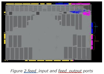
    In figure 2, the top ports that are pink in color represent the feed_input ports and feed_output port on the right bottom side. Similarly, for the blue color top right side is feed_output and the right one is the feed_input port. Instances that are highlighted in blue and pink color are registers.


      In figure 3, the Top right feed_input ports which are in blue are interacting with the feed_output port which is green in color and is placed on the right edge of the bland we see there are one pipeline registers between them which are shown by the yellow color line.


Implementation:


    As shown in figure 4, right-side feed_input* ports are swapped with feed_output* ports to improve congestion by reducing criss-cross near the ports. After implementing this Congestion improved from 4.4% to 2.2%.


Case 2: Fixing Register to output (REG2OUT) setup violation:

    At the floorplan stage, Macro/IP placement, pin/port placement, and power planning are performed. Only setup violations would be reported at the placement stage and hold violations will be reported after the CTS stage PNR flow.

    Path groups would be created for the timing path. This enables reporting the timing results separately for each group, as well as set the options to focus the timing optimization on specific critical timing path groups.

    Command (in Innovus) createBasicPathGroups – expanded can be used to create reg2reg, reg2Cgate, in2reg, reg2out, and in2out path groups.


    In the above figure path between flip-flop 1 and flip-flop, 2 is called as reg2reg path, and the path between flip-flop 2 and the output port is called as reg2out path. The reg2reg and reg2cgate default path groups are high effort path groups for optimization and the remaining path groups are low effort, path groups.

    We can also create custom path groups according to the requirement. STA person would define constraints for I/O timing e.g. input delay, external delay, etc. in the Synopsys design constraint (SDC) file. Virtual clocks are defined to constrain the I/O timing paths. While doing PnR at the block level, I/O timing should be met even though internal timing has a higher priority.

    While doing timing optimization, the tool will locate flip-flops according to timing requirements. As internal timing has a higher priority, it might be possible that the tool would place flip-flops a little away from the I/O port.

METHODOLOGY: -

    To fix the IO timing violation, we need to analyze the cause of the timing violations so that it can be fixed at the right stage. In this design, reg2out setup violation is reported at the placement stage. The tool placed those flops a little away from the output port to meet the internal timing. These violations need to be addressed at the placement stage itself. It was found that there was enough margin in previous timing paths (reg2reg). So flopbound could be created near the output port to fix the reg2out setup violations. Now there are a few things that need to be identified: -

  1. location of the bound
  2. Size of the bound
  3. Which group should be created out of soft Guide, Guide, Region, and Fence?

PNR tool, Innovus support four types of physical floorplan constraints namely soft guide, guide, region, and fence.

Implementation:


    In the design, a region of 48 flops has been created near the output port and it would prevent the spreading of those flops. Hence, reg2out setup violations can be reduced to the desired limit.

Specification of block

Dimension

2126 x 976.68

Instances

1.06 M

Utilization

17%

Macro count

220


    In the figure shown above, the output port has been highlighted and the placement of the registers has been shown before creating the region.


    In this figure, the location of the region has been shown in the design. It makes sure that internal timing should not get violated while fixing reg2out timing violations. Reg2out setup timing violation was reduced to the desired limit after implementation of the above methodology.

Thank you!

Tuesday, August 9, 2022

How Delay Calculation is Performed in POCV using Timing Report


What is POCV?

  • POCV stands for Parametric On-Chip Variation. It is an enhanced variation methodology over AOCV.
  • POCV advance variation technology provides statistical benefits without expansive statistical library characterization overhead.
  • POCV is very effective in technology nodes 20nm and below.


In POCV, instead of applying a specific derating factor to an individual instance, it models delay as a function of a random variable that is specific to that instance.

Delay = Delay (Nominal_Delay) + Delay (Delay_Variation) * P

Where,

P = Standard Normal Variable

Delay_variation (σ) for each cell is obtained through HSPICE simulation and it is a unique value specific to that library cell.

HSPICE = H(Hewlett)-Simulation Program with Integrated Circuit Emphasis; Hspice is a circuit simulator. It can take input circuit description files and produce output files describing the requested simulation.


In normal distribution 68% of data falls within the 1
σ range, 95% of data fall within 2σ and 99.7% of data fall within the range of 3σ. 

POCV uses a nominal value for modeling random variations on the die instead of using min-max delay values for the timing arc.

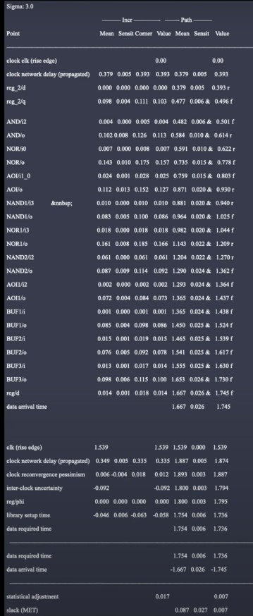
POCV analysis uses nominal delay (µ) and variation (σ) for timing analysis in the following way:

  1. The tool takes the value of σ from the timing library or an external file containing POCV coefficient C.
  2. Each arc timing is then calculated statistically as the total of the nominal delay and the variation.
  3. The tool then calculates the delay of the path by statistically combining these arc delays.

By default, the tool performs POCV analysis at three standard deviations (3σ) from the mean.


POCV DATA TYPES:

Single Coefficient (C): An external file contains the coefficients for the delay variations. It applies a single coefficient value C for each library cell, hierarchical cell, or design. The coefficient is the value of the variation at 1 standard deviation from the nominal delay. There is only one value of C for each timing arc of the cell irrespective of the input transition and output load.

                                        Delay variation (σ) = C * Nominal Delay

Below shows an example of POCV coefficient file:


Library Variation Format (LVF):

LVF is an extension to the Library Format (.lib) that adds statistical variations information to timing measurements.

  • POCV variation is directly provided in the library itself.
  • The variations are loaded in the design by loading the library. It contains the value of variation for multiple slew-load conditions of the cell instead of a single value of C.
  • The accuracy of the design at nodes < 16nm is greatly improved.
  • Similar to cell delay check, LVF supports POCV coefficients for transition and setup, hold checks as well.

An example of the POCV LVF format has shown below:
A


POCV Delay Calculation:

Delay of a cell = Nominal Delay +/- Variation


Delay of a cell = Nominal Delay +/- (C * Nominal Delay) * N

    Here, C = POCV coefficient; N = No. of STD deviations


Sensitivity = Mean * POCV coefficient (C)


Corner = Mean +/- (N * sensitivity) ; N = No. of STD deviations


Incr value = Current stage path value – Previous stage path value


Mean for path column = Mean (1st stage) + mean (2nd stage) ….mean (cur stage)


Sensitivity for path column = sqrt [ sens_1st_stg^2 + sens+2nd_stg^2 + …. + sens_cur_stg^2]


Path value = Path mean + (Path sensitivity * N)


For Incr:

Mean = 0.102                                                    

Sensit = Mean * C

            = 0.102 * 0.0784

            = 0.008

Corner = Mean + (N * Sensit)

             = 0.102 + (3 * 0.008)

             = 0.126

Value = Curr stg value – Prev stg value

           = 0.614 – 0.501

           = 0.113


For Path:

Mean = 0.379 + 0.000 + 0.098 + 0.004 + 0.102

          = 0.584

Sensit = sqrt[(0.006 * 0.006) + (0.008 * 0.008)]

            = 0.010

Value = Mean + (Sensit * N)

           = 0.584 + (0.010 * 3)

           = 0.614

  •          POCV models random variation.
  •          Use AOCV derating along with POCV to model systematic variations.


To model non-process-related variations such as voltage and temperature. It applies to both nominal delay and sigma.

When both derates (distance-based and guard band) are present then derate will be the product of the two.

POCV distance derate * POCV guard band

Summary:
In this article POCV has been discussed in detail, The aim of this article is to provide the basic concept of POCV and how to delay calculate using timing report and give a comparative insight. 

Thank you!

How IR Drop does affect the Timing?

  IR Drop is Signal Integrity (SI) effect caused by wire resistance and current drawn off from Power (Vdd) and Ground (Vss) grids. According...